Tiny Nanoscale Filaments Could be Breakthrough for Smaller, Denser Memory Devices
From the Journal: AIP Advances
WASHINGTON, D.C. Sept. 20, 2013 — Memory based on electrically-induced “resistive switching” effects have generated a great deal of interest among engineers searching for faster and smaller devices because resistive switching would allow for a higher memory density.
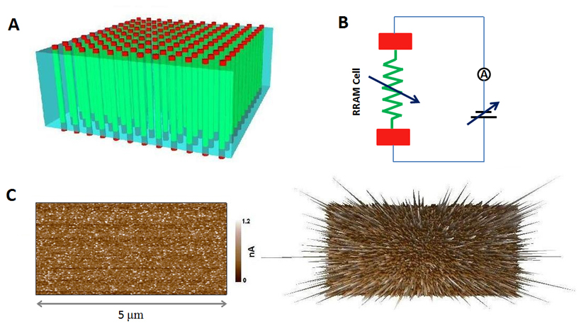
Researchers have tested a number of oxide materials for their promise in resistive switching memories, and now a team of researchers in Singapore have demonstrated how conductive nano-filaments in amorphous titanium dioxide (TiO2) thin films could be utilized for resistive switching device applications.
Yuanmin Du, Andrew Thye Shen Wee and researchers from the National University of Singapore and the Agency for Science, Technology and Research (A*STAR) of Singapore, describe their results in the journal AIP Advances, which is produced by AIP Publishing.

How Resistive Switching Works
The basic idea of a resistive switching device is that an oxide, which normally acts as an insulator, can be transformed into a conductor, creating a nanoscale filament by using a sufficiently high voltage. With a RRAM (Resistive Random-Access Memory) device comprising of a single filament, two distinct resistance states (“1” and “0”) can be obtained through a simple process of filament rupture and re-formation.
The conductivity of the oxide thin films can be adjusted by changing the deposition conditions. “During the measurements of the as-deposited amorphous TiO2 based resistive switching devices, it was found that the oxide thin films initially have good conductivity. This implies that a high electrical breakdown initialization process is not required, as reported in many other switching devices using highly insulating oxide thin films”, says Du. “The Conductive Atomic Force Microscopy (CAFM) experiments further confirmed that it is possible to form conductive filaments in oxide thin films through a localized transition by an electrical field.”
This research team applied both CAFM and KPFM (Kelvin Probe Force Microscopy), a unique approach that allowed the explanation of the observed resistive switching phenomena. Instead of treating filamentary and interfacial effects separately as done previously, both effects were integrated into one filament-interface model, which could help guide the design of RRAM based devices.
The evidence of high density and uniformly distributed nano-filaments implies that high-density memory cells could be made using such oxide thin films. Such materials are promising for future applications. The small dimension of the formed filament provides great advantages over current technology, as Du explains. “In addition to TiO2, we believe that many other oxides could also have the similar properties.”
###
For More Information:
Jason Socrates Bardi
jbardi@aip.org
240-535-4954
@jasonbardi
Article Title
Authors
Yuanmin Du, Amit Kumar, Hui Pan, Kaiyang Zeng, Shijie Wang, Ping Yang and Andrew Thye Shen Wee
Author Affiliations
National University of Singapore and Agency for Science, Technology and Research (A*STAR) of Singapore
