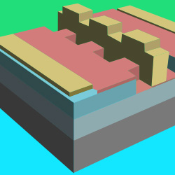
Critical Issues on the 2D-material-based Field-effect Transistors
 The Si complementary metal oxide semiconductor (CMOS) technology has followed the Moore’s Law to scale the size and thickness of active channels, but it becomes very challenging when Si approaches the physical limit. The ultimate channel thickness for a field-effect transistor (FET) would be in the sub-1 nm range, which is not readily accessible for any three-dimensional (3D) semiconductors. The semiconducting 2D materials with an ultra-thin body and smooth surfaces have great potential and are being seriously investigated as post-Si electronic materials. Field-effect transistors based on two-dimensional (2D) materials have been studied for many years and have shown the potential to serve future large-scale integration (VLSI) technologies. However, it remains to be determined whether 2D materials can be used in the front end to replace or parallel the Si channel. Meanwhile, there is a growing trend to integrate transistors based on 2D materials with silicon devices through monolithic or heterogeneous integration to increase the functionality of existing silicon chips. Meanwhile, applications of 2D transistors in digital and analogue electronics, memory, neuromorphic computing and sensing devices are also considered promising. To help achieve these goals, many significant challenges need to be addressed. In this special issue, we hope to solicit relevant submissions that focus on but are not limited to, the above-mentioned topics, in order to promote the further development of the nominated research field.
Topics covered include, but are not limited to:
- Choice of suitable 2D materials, and doping methods for p- and n-channels,
- Strategies to reducing the contact resistance of metal-2D materials,
- Strategies to reducing charge traps at the interface of dielectrics and 2D materials
- Mobility engineering in 2D materials,
- Improving high-κ dielectrics for scaling
- Development of large-area growth and damage-free transfer processes
- Strategy to construct 2D transistors in back-end-of-line processes
- Simulation for 2D devices and circuits
- Applications of 2D transistors in digital and analogue electronics, memory, neuromorphic computing and sensing devices
Author Information
For details on the scope and criteria of Applied Physics Letters, please see the journal’s Editorial Policies. For guidelines on manuscript preparation, including manuscript length, please see the journal’s Author Instructions.
Guest Editors
Lain-Jong Li, University of Hong Kong
Qiming Shao, Hong Kong University of Science and Technology
Mario Lanza, King Abdullah University of Science and Technology
Yang Chai, Hong Kong Polytechnic University
Taishi Takenobu, Nagoya University
APL Editors
Minn-Tsong Lin, National Taiwan University
