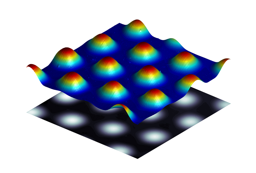
TU Darmstadt researchers pattern large areas with highly regular structures in a single process step that involves generating structures from a liquid -- ideal for fabricating microlens arrays for advanced photovoltaic systems.
From the Journal: Applied Physics Letters
WASHINGTON, D.C., February 11, 2016 – Have you ever noticed that when heated a film of oil in a pan doesn’t remain completely flat? Instead, it forms a wavy pattern that resembles the exterior of an orange. These sorts of deformations inspired a group of researchers at the Technical University of Darmstadt, in Germany, to explore whether they could be used to improve and streamline microfabrication processes.
The film of oil is a classic example of a hydrodynamic systems with a liquid-gas interface while, for instance, the tiny droplets of fat in milk have a liquid-liquid interface. Planar liquid films, like the oil film, are particularly mechanically unstable and may undergo changes in morphology if not kept at a uniform temperature.
Only sufficiently thin liquid films undergo significant surface deformations upon exposure to stresses at the surface, while highly regular periodic flow patterns develop in the bulk of thicker films when subjected to the same stresses.
In marked contrast to thinner films, thicker films don’t show significant surface deformations. So, in the context of developing unconventional microfabrication techniques, most efforts have focused on the interfacial instabilities of very thin films.
These efforts indicated that accentuated patterns can be achieved, but they are unfortunately highly irregular in the spread direction of the film. This fundamental drawback can be traced to the same reason a water jet running from a faucet eventually splits up into droplets: surface tension.
As the group describes in Applied Physics Letters, from AIP Publishing, they combined the highly regular convection pattern that forms in thicker layers with strong interfacial deformations possible only in much thinner liquid films. “Unlike previous work addressing systems with several interfaces, in our approach each layer has a vastly different initial thickness than the other,” said Iman Nejati, the paper’s lead author and a Ph.D. student at the Institute for Nano and Microfluidics, Center of Smart Interfaces, TU Darmstadt.
This approach essentially involves sandwiching a thin film of oil that’s sensitive to irradiation with ultraviolet (UV) light between a solid planar substrate and a much thicker layer of another immiscible liquid. This implies that the system has not only a liquid-gas interface as the initial example of the oil film in a pan but also a liquid-liquid interface.
“Exposing this multilayer system to a surprisingly small temperature difference in the direction of the layering causes stresses at the liquid-gas interface because of a temperature-dependent surface tension,” said Nejati. “These stresses drive rotating cellular flow patterns in the thicker layer, which are highly periodic in the spread direction of that layer.”
Rather than using the stresses caused by the temperature-dependent surface tension directly to pattern the film, the group’s approach relies on the flow pattern in the thicker layer to deform the thinner film beneath.

This strategy enables “patterning large areas with highly regular structures in a parallel fashion — all structures are fabricated at the same time — in a single process step, which saves time and reduces costs,” explained Nejati. “Since the structures are generated from a liquid, without tools making mechanical contact with the working material, the surface is very smooth and doesn’t require any further processing.”
And by engineering the temperature distribution along the liquid-gas interface of the thicker layer, the convection cells and deformation of the thin film can be adapted to meet the specifications of a desired structure of interest. Once the desired deformation is achieved, it’s “frozen” in place by irradiation with UV light.
The combination of the named advantageous features of the new technique are highly desirable because all common microfabrication technologies — including photolithography, printing, or embossing — fail to meet at least one of these criteria. “Given the relative simplicity of the equipment needed for our method, and how easily it adapts to specific situations, it can be used for manufacturing low-quantity products as well,” Nejati added.
What applications does the group envision for their method? For starters, it’s ideal for fabricating microlens arrays. “These arrays locally enhance light intensity and can be used by the optics industry in integral imaging systems, unconventional photolithography, and photovoltaic systems,” explained Nejati. “For photovoltaics, an array of lenses placed atop a solar cell can serve as a light collector to enhance the efficiency of the photovoltaic system by making it less sensitive to the inclination angle of the solar light with respect to the cell surface.” The group’s method could easily be integrated into the manufacturing process of solar cells.
In the near future, “there will be no direct need to solidify the structures by UV light,” he noted. “Instead, the array of lenses can remain in the liquid state, which allows us to change the periodicity of the liquid lenses if, say, the temperature difference driving the convection cells is varied. This should contribute to the development of tunable lens arrays.”
###
For More Information:
Jason Socrates Bardi
jbardi@aip.org
240-535-4954
@jasonbardi
Article Title
Exploiting cellular convection in a thick liquid layer to pattern a thin polymer film
Authors
Iman Nejati, Mathias Dietzel and Steffen Hardt
Author Affiliations
Technische Universität Darmstadt (TU Darmstadt)
