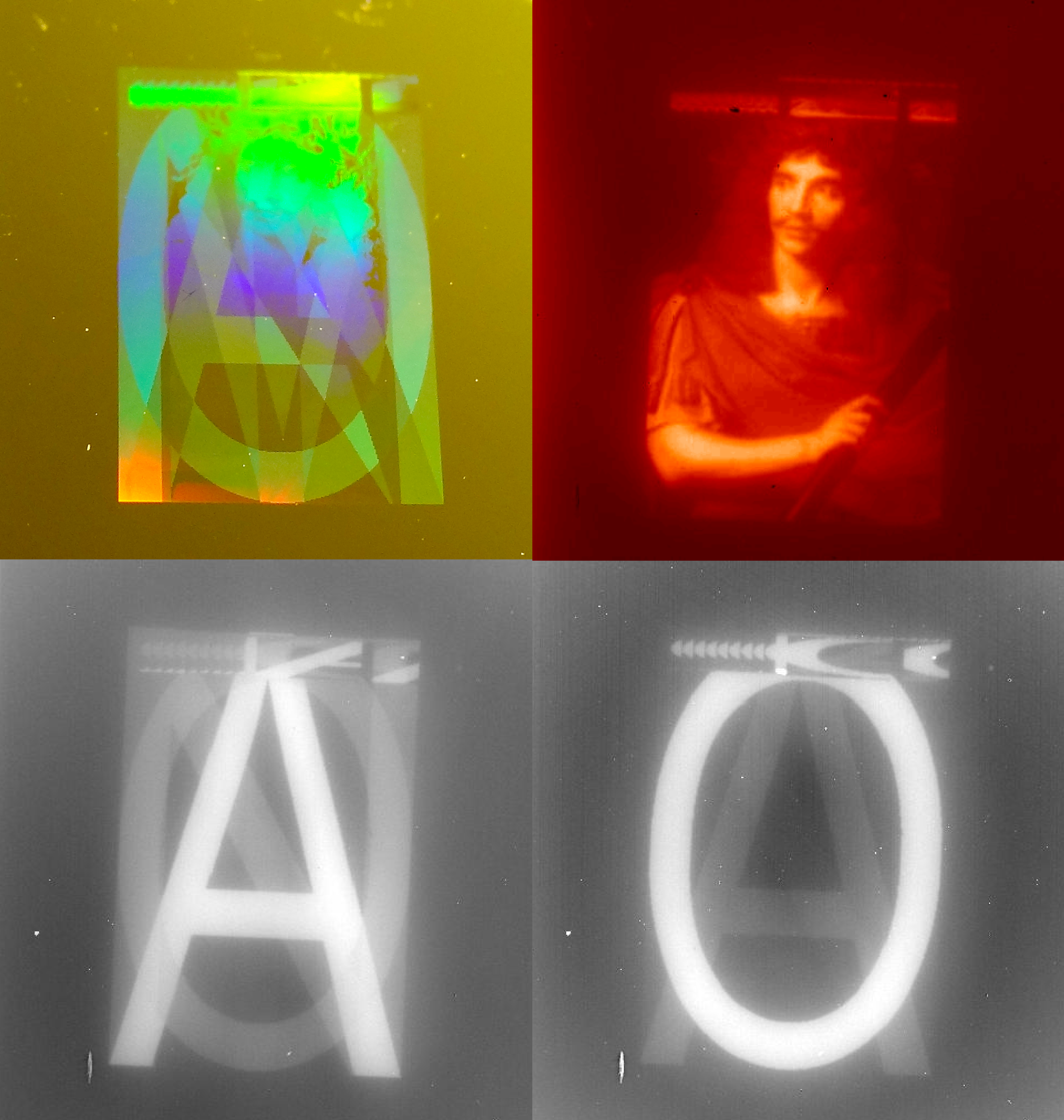
French researchers have demonstrated subwavelength control of thermal emissivity at the subwavelength scale – allowing them to encode images in infrared signals
From the Journal: Applied Physics Letters
WASHINGTON, D.C., December 22, 2015 – Researchers at MINAO, a joint lab between The French Aerospace Lab in Palaiseau and the Laboratoire de Photonique et de Nanostructures in Marcoussis, have recently demonstrated metamaterial resonators that allow emission in the infrared to be tuned through the geometry of the resonator.
Their setup uses sub-wavelength scale metal-insulator-metal, or MIM, resonators to spatially and spectrally control emitted light up to its diffraction limit. This allows an array of resonators to be used to form an image in the infrared – much as way the pixels in a television screen can form a visible light image – with potential breakthrough applications in infrared televisions, biochemical sensing, optical storage, and anti-counterfeit devices.
“MIM metasurfaces are great candidates for infrared emitters thanks to their ability to completely control thermal emission, which is groundbreaking compared to the usual thermal sources, such as a blackbody,” said Patrick Bouchon, a researcher at The French Aerospace Lab, also known as ONERA. “Moreover, this study shows the possibility to create infrared images with the equivalent of visible colors.”
Bouchon and his colleagues detail their work this week in Applied Physics Letters, from AIP Publishing. The researchers previously demonstrated the ability to manipulate light through tailoring its absorption or converting its polarization, and have investigated the “funneling effect,” in which incoming light energy is coupled to a nanoantenna.
Much as its name implies, a metal-in-metal, or MIM, nanoantenna consists of a rectangular metallic patch on top of an insulating material, atop another metallic layer. According to Bouchon, most metasurfaces – the aggregate of many nanoantennas on a substrate – are periodic repetitions of a given pattern, and exhibit no spatial modulation. Additionally, the idea of modifying the emissivity with nanostructures is relatively recent – the possibility to combine several antennas in the same subwavelength period was first shown by their team in 2012.
For their MIMs, Bouchon and his colleagues deposited 50 nanometer-thick rectangular patches of gold on top of a 220 nanometer silicon oxide layer, which sat atop an opaque 200 nanometer gold layer.
“We had to theoretically predict the response of 100 million antennas, and to subsequently fabricate it,” said Mathilde Makhsiyan, a PhD student at The French Aerospace Lab. To do this, the researchers developed their own electromagnetic software, as well as specific software to generate the e-beam files for the fabrication of spatially modulated emissivity metasurfaces.
Once fabricated, each nanoantenna acts as an independent deep subwavelength emitter for a given polarization and wavelength. This allows it to control emission properties such as wavelength, polarization, and intensity with its specific geometry and orientation. When juxtaposed on a large scale, these MIMS cause the emissivity to be defined at the sub-wavelength scale, allowing the researchers to encode several images on the same metasurface.
This emission information is encoded in a unit cell that has a size smaller than that of the wavelength, on account of the effect of the antennas’ varied geometries and orientations on how the information is encoded. Because of this, two neighboring cells can possess different encoded information and encode the information spatially. This ultimately allows for the creation of a static infrared image, similar to an LCD screen.
Future work for Bouchon and his colleagues includes independently controlling each of these pixels to create a dynamic emission of light – a first step towards an infrared TV – as well as creating a start-up business to develop anti-counterfeit devices.
###
For More Information:
Jason Socrates Bardi
jbardi@aip.org
240-535-4954
@jasonbardi
Article Title
Shaping the spatial and spectral emissivity at the diffraction limit
Authors
Mathilde Makhsiyan, Patrick Bouchon, Julien Jaeck, Jean-Luc Pelouard and Riad Haidar
Author Affiliations
MINAO, a joint lab between The French Aerospace Lab (ONERA) in Palaiseau and the Laboratoire de Photonique et de Nanostructures in Marcoussis
