A France-U.S. research team's new spin on MRAM technology led to a multi-bit storage paradigm that may rival flash memory storage
From the Journal: Applied Physics Letters
WASHINGTON D.C., July 22, 2014 — Interest in magnetic random access memory (MRAM) is escalating, thanks to demand for fast, low-cost, nonvolatile, low-consumption, secure memory devices. MRAM, which relies on manipulating the magnetization of materials for data storage rather than electronic charges, boasts all of these advantages as an emerging technology, but so far it hasn’t been able to match flash memory in terms of storage density.
In the journal Applied Physics Letters, from AIP Publishing, a France-U.S. research team reports an intriguing new multi-bit MRAM storage paradigm with the potential to rival flash memory.
Increasing the density of memory devices is highly desirable and can be accomplished via a variety of methods. One way is by reducing the patterning dimensions, which leads to an increased number of memory cells per unit surface. Another approach involves increasing the storage capacity of each individual cell — aka “multi-bit storage.”
“Multi-bit storage is typically achieved in MRAM technology by measuring the multiple voltage levels corresponding to various magnetic configurations,” explained Quentin Stainer, lead author of the paper and a Ph.D. student at SPINTEC/CEA, a research institute for electronics and information technologies located in Grenoble, France, and also affiliated with Crocus Technology, a France- and U.S.-based firm that develops magnetically enhanced semiconductor technologies.
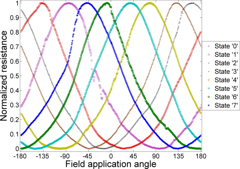
At the heart of the team’s work is Crocus Technology’s proprietary Magnetic Logic Unit (MLU) technology, which enables the researchers to remotely control a sensor to probe these configurations. “By identifying key features of the electrical responses we obtain, typically known as ‘extrema points,’ we can infer the stored information,” Stainer said.
The highlight of their work was the “unambiguous demonstration of the feasibility of our method, with as much as 3 bits per unit cells, and recently up to 4 bits, obtained on 110-nanometer-wide devices,” he noted.
It’s also worth noting that the team says their storage paradigm should be able to provide an increased robustness and tolerance to process variability, which will make it easier to produce devices based on this technology for industrial applications.

“Our work will enable the development of products for a wide range of applications including, but not limited to, secure data storage for connected devices — such as smart card, content-addressable memory for Internet routers, as well as high-performance, high-density, and high-temperature memory,” Stainer said.
The team’s next step? Developing a fully functional multi-bit MLU memory product to further demonstrate the industrial viability of their storage paradigm. “New memory paradigms derived from this work are also under development — with potential multi-bit capacities of up to 8 bits per single cell,” he added.
This work was supported by a contract (N66001-13-C-2003) from the U.S. Office of the Director of National Intelligence’s IARPA (Intelligence Advanced Research Projects Activity) group.
###
Article Title
Self-referenced multi-bit thermally assisted magnetic raandom access memories
Authors
Q. Stainer, L. Lombard, K. Mackay, D. Lee, S. Bandiera, C. Portemong, C. Creuzet, R.C. Sousa, and B. Dieny
Author Affiliations
SPINTEC/CEA and Crocus Technology
